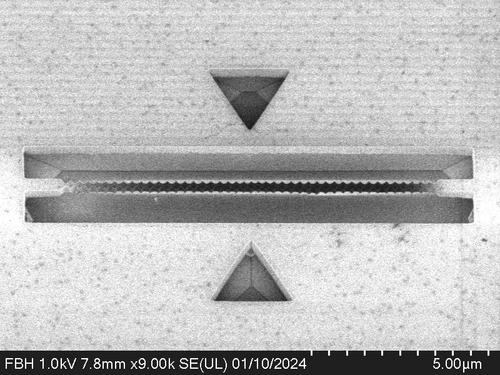
Electron microscope image of a Sawfish Cavity: Top view of the tiny diamond structure. The design and simulation are by Julian Bopp, and it was manufactured by Marco Stucki.
In the hope that the wider research community would try out our structure, we wanted to find a name that would be easy to remember. The nose of the sawfish is reminiscent of the wave-like pattern of our structure. The name is short, snappy, and sticks in your mind.
You work with diamonds on a nanoscale—how can we imagine that?
Our cavity is about one hundredth of a millimeter long, but ideally only 20 millionths of a millimeter wide. If you were to shrink the entire city of Berlin to the width of a human hair, the width of the cavity would be about the size of the ball on the TV tower. Working with diamonds on this scale is an additional challenge because it is the hardest material in the world and can only be scratched by another diamond. Chemically, diamonds are non-reactive, so strong acids and bases cannot damage them.
How do you create such small structures in such a hard material?
With plasma. We use technologies developed by the semiconductor industry to manufacture microchips. Put simply, we apply a kind of lacquer to the diamond.

